


LED Display Technology
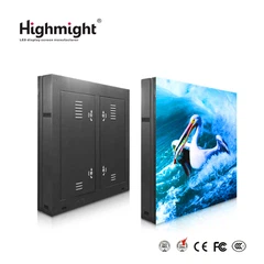
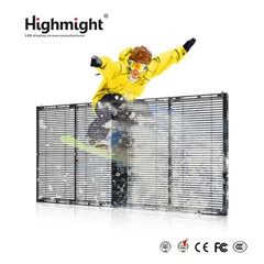
After being packaged, LED beads are arranged in a fixed pattern on a PCB (Printed Circuit Board) to form an LED light array. This unit, along with the peripheral driver circuitry, is called an LED module (also known as an LED board). Multiple LED modules, combined in a regular pattern, along with a receiver card and power supply, form a unit called an LED cabinet. An LED display, constructed by arranging multiple LED cabinets, cannot illuminate the display to display valid content. A dedicated controller and video source are required.
The video source can come from a computer, player, media server, camera, or other device. These devices output the video source to an LED controller, which decodes the video source, converts the format, and cuts the image. The controller then outputs the final data format suitable for the LED display to the receiver card within the LED cabinet. The receiver card then controls the brightness and color of the LED chips, thereby displaying the desired content on the LED display. Figure 1-2-1 shows the topological system structure of an LED display. From the perspective of the entire LED display structure, LED display technology includes LED display control system technology, LED drive technology, LED display correction technology, LED packaging technology, LED light-emitting chip technology, etc.

LED Display Industry Chain Structure
The various technical links of LED displays are closely integrated to form the LED display industry chain. This industry chain is divided into three segments: the chip end (upstream), the packaging end (midstream), and the display end (downstream), as shown in the figure.

The chip side primarily refers to epitaxial wafer production, specifically the LED chips and related materials, which is the manufacturing process for LED chips. The technology required for this endeavor encompasses fundamental knowledge in chemistry and physics, resulting in a high technical barrier to entry and a significant influence on the development of the entire LED display industry chain.
The packaging side primarily refers to the packaging of LED chips, specifically the assembly of ED chips into individual pixel units. Products typically involved in this process include DIP-packaged LED units and SMD-packaged LED pixels. This process uses specialized process technologies to shape the chip-side products into a form that facilitates handling and soldering.
The display side primarily refers to finished LED displays, namely LED display modules, LED enclosures, and LED screens. This segment involves a wide range of industries, including driver chips, power supplies, control systems, and hardware enclosures.
Key Technology Development Timeline
LED displays have evolved from ultra-large outdoor pitch to fine indoor pitch, and now to ultra-fine indoor pitch. The main reason for this is that early LED light-emitting semiconductors suffered from low luminous efficiency and a single color display, limiting their application to simple display applications, such as text-only doorway advertisements and traffic signs displaying symbols and simple colors. Only after the efficiency issue was resolved did LED displays enter the full-color era. However, at the time, the dot pitch of LED displays was still very large, primarily used for outdoor advertising, information notices, and other applications requiring ultra-long-distance viewing.
With technological advancements and the emergence of SMD packaging technology, LED display dot pitches have been able to reach P3.9 or even P2.5. This allowed LED displays to be installed in outdoor venues with close viewing distances, such as concerts and community plazas, and some even began to be used indoors. When the dot pitch of LED displays reached P2.0 or below, LED displays became common in many indoor locations, such as shopping mall escalators, store entrances, and corporate showrooms. Continuous technological innovation is driving the development of LED displays and their entry into new fields. Different dot pitches bring different application scenarios, requiring different technologies and solving different problems.

LED Chip Technology and Its Developments
The principle of LED light emission is simple. First, an LED chip must have a PN junction. The P region is primarily holes, while the N region is primarily electrons. The point where the P and N regions meet is called the PN junction. Secondly, when the forward bias voltage is increased, the carriers in the P and N regions disperse toward each other, causing electrons and holes to migrate. At this point, the electrons and holes recombine to generate energy, which is converted into photons and emitted. The color of the light emitted is primarily determined by the wavelength of the light, which is determined by the material of the PN junction.

Over the course of LED development, chip technology has undergone numerous innovations and evolutions. Initially, due to process technology limitations, the PN junctions of LED chips were large, indirectly impacting the size of LED beads. With the continuous advancement of process technology and LED chip structure, LED chips have become increasingly smaller, even reaching sizes of 100μm and below.
Currently, there are three main LED chip structures. The most common is the face-up structure, followed by the vertical and flip-chip structures, . The face-up structure is the earliest chip structure and is also commonly used in LED displays. In this structure, the electrodes are located at the top, with the following sequence: P-GaN, multiple quantum wells, N-GaN, and substrate. The vertical structure uses a high-thermal-conductivity metal substrate (such as Si, Ge, and Cu) instead of a sapphire substrate, significantly improving heat dissipation efficiency. The two electrodes in the vertical structure are located on either side of the LED epitaxial layer. Through the N electrode, current flows almost entirely vertically through the LED epitaxial layer, minimizing lateral current flow and preventing localized overheating. From top to bottom, the flip-chip structure consists of a substrate (typically a sapphire substrate), N-GaN, multiple quantum well P-GaN, electrodes (P and N electrodes), and bumps. The substrate faces upward, and the two electrodes are on the same side (facing downward). The bumps are directly connected to the base (sometimes called a substrate, such as a PCB substrate) downward, greatly enhancing the core's thermal conductivity and providing higher luminous efficiency.
LED Packaging Technology and Its Development
Packaging is an essential step in the development of LED displays. Its function is to connect the external leads to the electrodes of the LED chip, while also protecting the chip and improving luminous efficiency. Good packaging can enhance the luminous efficiency and heat dissipation of LED displays, thereby extending their lifespan. Throughout the development of LED displays, the packaging technologies that emerged in sequence are DIP (Dual In-line Package), SMD (Surface Mount Device), IMD (Integrated Matrix Device), COB (Chip-on-Board), and MIP (MicroLED In Package).
Displays using DIP packaging technology are often referred to as direct-insert displays. LED lamp beads are manufactured by lamp bead packaging manufacturers and then inserted into the LED PCB by LED module and display manufacturers. Wave soldering is then performed to create DIP semi-outdoor and outdoor waterproof modules.

Displays using SMD packaging technology are often called surface-mount displays. This packaging technique encapsulates three RGB LEDs within a single cup to form one RGB pixel. Full-color LED displays produced with SMD packaging technology offer a wider viewing angle than those produced with DIP packaging technology, and the surface can be treated for diffuse light reflection, resulting in a much less grainy effect and excellent brightness and color uniformity.
Displays using IMD packaging technology are often called all-in-one displays. IMD packaging technology encapsulates multiple RGB pixels within a large cup, essentially falling under the umbrella of SMD packaging. In addition to leveraging existing SMD process technology, IMD packaging allows for a very small pixel pitch, breaking through the existing SMD packaging barrier.
Displays using COB packaging technology first solder the LED chip directly to the PCB and then seal it with a layer of resin adhesive. COB packaging eliminates the SMD process of encapsulating the RGB LED chips within the cup to form individual pixels, and also eliminates the mixing of LEDs required with SMD packaging. Therefore, COB packaging technology suffers from poor display uniformity, requiring LED display calibration technology to address this. However, COB packaging technology is closer to surface light sources, with each pixel boasting a very wide light output angle, excellent protection, and the ability to achieve a very small pixel pitch.
MIP packaging technology is actually more of an intermediate between SMD and COB packaging technologies. It involves placing the LED chip on a PCB, then cutting the PCB into individual pixel sizes. This allows for mixed lighting similar to SMD packaging, ensuring inherent uniformity while also ensuring protection.
LED Driver Technology and Its Development
Driver chips are generally referred to as driver ICs. Early LED displays were primarily single- and dual-color, utilizing constant-voltage driver ICs. In 1997, my country introduced the first dedicated driver IC for full-color LED displays, expanding from 16 grayscale levels to 8192. Subsequently, constant-current drivers became the preferred driver for full-color LED displays, driven by the unique characteristics of LED lighting. At the same time, more integrated 16-channel drivers replaced 8-channel drivers. In the late 1990s, Japanese companies such as Toshiba and American companies such as Allegro and T successively launched 16-channel LED constant-current driver ICs. In the early 21st century, Chinese companies also began mass-producing and using these driver ICs. Today, to address the PCB wiring issues of fine-pitch LED displays, some driver IC manufacturers have launched highly integrated 48-channel LED constant-current driver ICs.
In the operation of a full-color LED display, the driver's role is to receive display data (from a receiving card) that complies with the protocol specifications and internally generate PWM (pulse width modulation) and current-time variations to output a PWM current related to brightness and grayscale refresh rates to illuminate the LEDs. LED driver ICs can be divided into general-purpose ICs and specialized ICs. General-purpose ICs are not designed specifically for LED displays, but rather chips that match some of the logical functions of LED displays. Dedicated ICs are designed based on the light-emitting characteristics of LEDs and are specifically designed for LED displays. The following diagram shows their architecture. LEDs are current-dependent devices, and their brightness changes with current. However, this current change can cause the wavelength of the LED light chip to shift, indirectly leading to color distortion. A key feature of dedicated ICs is their ability to provide a constant current source. This constant current source ensures stable LED drive, eliminating flicker and color distortion, and is essential for high-quality image quality on LED displays.


The above driver IC approach is called PM (Passive Matrix) driving, also known as passive driving or passive location-based driving. With the emergence of Micro LED and Mini LED, the dot pitch of displays continues to shrink, increasing the density of driver components and complicating PCB wiring. This impacts display reliability, driving driver ICs towards higher integration and, in turn, higher scan counts. However, the higher the scan count of PM driving, the worse the display quality.
AM driving, also known as active driving or active location-based driving. Comparison between AM and PM driving. From a human perspective, AM driving appears flicker-free and is more comfortable for the eye. It also consumes less power. Furthermore, AM driving, due to its higher integration density, requires fewer chips.

LED Display Control System Technology and Its Development
LED display control systems are key to achieving excellent image quality, and image quality improvements are largely achieved through the control system. A basic control system consists of control software (host computer software), a controller (independent master control), and a receiver card. The control software primarily configures various display parameters; the controller primarily performs image segmentation on the video source; and the receiver card outputs the video source sent by the controller according to a specific timing sequence, thereby illuminating the entire display.
Controller Development History
Control systems, serving as the "central system" of LED displays, initially appeared in the form of boards, with typical products such as Nova Nebula's MSD300. Later, as display pixel pitches and application scenarios evolved, chassis-based controllers gradually emerged, with typical products such as Nova Nebula's MCTRL600. Later, as LED displays entered indoor and small rental applications, there was a demand for simple display adjustments, and the controller form factor evolved, adding front-panel LCD debugging capabilities. Typical products include Nova Nebula's MCTRL660. As display pixel pitch continues to shrink, the number of 4K displays on the market is increasing. This has increased the load capacity of a single controller, requiring a controller capable of directly handling 4K resolution. Consequently, 16-port controllers have emerged, with a typical example being the Nova Nebula MCTRL4K. As display pixel pitch continues to shrink and application scenarios expand, the performance requirements for controllers are also increasing. Controllers with video processing capabilities are emerging, with typical products such as the Nova Nebula V700, V900, and V1260. Some projects also require large-screen splicing capabilities, leading to the emergence of controllers with both splicing and video processing capabilities. Typical products include the Nova Nebula H2, H5, and H9 series splicing controllers.

The Development of Receiver Cards
In the history of receiver cards, since LED displays were initially primarily used outdoors, for ease of installation and maintenance, most receiver cards featured built-in hub interfaces, such as the Nova Nebula DH426. As LED displays transitioned from outdoor to indoor use, requirements for image quality, bandwidth, and structure became increasingly stringent. This led to the emergence of receiver cards with high-density interfaces, resulting in smaller sizes, such as the Nova Nebula Armor series. With the emergence of new pixel pitch and packaging technologies, LED displays have been increasingly used in high-end applications such as home theater, education, and healthcare, placing higher demands on control systems. These demands require not only higher image quality but also higher frame rates to ensure a better and more realistic representation of the world. This necessitates higher-bandwidth receiver cards, such as the Nova Nebula CA50 5G receiver card.
With the advancement of Mini LED and Micro LED technologies, the requirements for LED displays are becoming increasingly stringent, demanding not only higher image quality and greater bandwidth, but also thinner, more ergonomic, and more flexible structural designs. This has necessitated the use of control chip-level receiver cards to meet these market demands.


