
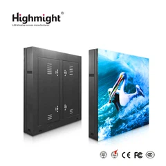


Overview of COBLED small pitch technology
In today's digital age, display technology is an important carrier of information transmission, and its development level is directly related to the quality of visual experience. In recent years, COBLED (Chip on Board Light Emitting Diode) small pitch display technology has emerged and quickly become a new favorite in the professional display field with its excellent performance. COBLED small pitch usually refers to LED display products with a pixel pitch below P1.5. This technology has achieved a major breakthrough in display technology by using an innovative process of directly encapsulating LED chips on circuit boards.
Traditional LED display screens use SMD (Surface Mounted Device) packaging technology, while COBLED uses a completely different technical path. COBLED technology eliminates the bracket and lead links in traditional LED packaging, directly fixes the LED chip on the PCB board, and then protects it with packaging materials. This technological change brings multiple advantages: higher pixel density, better thermal conductivity, stronger environmental adaptability and longer service life.
From the technical principle point of view, COBLED small pitch display screens are composed of tens of thousands of micro LED chips directly encapsulated, and each LED chip is controlled to emit light as an independent pixel through a precise driving circuit. When the pixel pitch is reduced to less than 1.5 mm, the human eye can hardly distinguish individual pixels at a normal viewing distance, thus achieving a nearly seamless visual experience. This high-density integration technology enables COB LED to demonstrate unparalleled advantages in high-end application scenarios such as conference rooms, command and control centers, and radio and television.
Core technical advantages of COBLED small pitch
The reason why COBLED small pitch technology has been highly recognized by the industry in a short period of time is due to its many core technical advantages. These advantages not only solve the pain points of traditional display technology, but also set new standards in the field of professional display.
Ultra-high pixel density and seamless display experience are the most notable features of COBLED. Due to the use of chip direct packaging technology, COBLED can achieve a pixel pitch of P0.4 or even smaller, providing higher resolution at the same size. Taking a 110-inch 4K display as an example, COBLED technology can easily achieve this specification, while traditional technology faces huge challenges. This high-density arrangement makes it completely invisible to viewers at a normal distance, which is especially suitable for occasions that require fine image display, such as medical imaging diagnosis, military command systems, etc.
Excellent color performance is another major advantage of COBLED. Traditional LED displays often have poor color consistency due to packaging materials and process limitations. COBLED technology uses unified packaging materials and precise chip screening to achieve professional-grade color accuracy of ΔE<2, covering more than 90% of the DCI-P3 wide color gamut. This means that COBLED display screens can accurately restore the original color of images and meet the needs of fields with extremely strict color requirements such as radio, television, and film post-production.
The revolutionary improvement of thermal management performance is another major breakthrough in COBLED technology. Due to the limitations of the packaging structure of traditional SMD LEDs, heat needs to be conducted through multiple interfaces, and the heat dissipation efficiency is low. COBLED directly solders the chip on a PCB board with excellent thermal conductivity, reducing thermal resistance by more than 60%. Measured data shows that under the same working conditions, the temperature of the COBLED module is 15-20℃ lower than that of the traditional SMD module, which not only extends the life of the device, but also significantly reduces the brightness decay rate, ensuring that the display maintains a stable light output for a long time.
In terms of reliability and environmental adaptability, COBLED also performs well. The metal leads of traditional SMD LEDs are prone to breakage in a vibrating environment, while the leadless structure of COBLED fundamentally solves this problem. After rigorous testing, COBLED modules can withstand multi-axial random vibrations of 5-500Hz, which is very suitable for mobile platform applications such as vehicles and ships. In addition, COBLED's integrated packaging structure enables it to have IP65-level dust and water resistance, and can operate stably in extreme environments of -40℃ to 85℃, meeting the needs of various harsh industrial environments.

Technical comparison between COBLED and traditional SMD
In-depth comparison of the differences between COBLED and traditional SMD technology will help us understand the revolutionary nature of COBLED technology more comprehensively. There are essential differences between the two technologies from material selection, process technology to performance, and these differences directly determine their applicability in different application scenarios.
From the perspective of packaging structure, SMD technology adopts a two-step process of first encapsulating LED chips individually and then installing the encapsulated devices on the PCB board through the patch process. COBLED simplifies this process and adopts an integrated process of "chip-solid crystal-wire bonding-mold sealing" to complete all packaging processes directly on the PCB board. The most direct impact of this structural difference is that the physical size of COBLED is smaller, and more pixels can be arranged on the same PCB area, which is the basis for realizing small-pitch display.
In terms of optical performance, the two technologies also show obvious differences. Since SMD uses an independent plastic bracket package, the light needs to pass through the packaging material to be emitted, and there is a certain amount of light loss and color deviation. COBLED adopts direct optical interface design. After the light is emitted from the chip, it only passes through a thin layer of packaging material, which increases the light efficiency by more than 20% and expands the viewing angle to more than 170 degrees. Actual tests show that the brightness of COBLED modules is 15-30% higher than SMD under the same current drive, and the color deviation within the viewing angle is reduced by more than 50%.
In terms of process technology, COBLED has higher requirements for production equipment and technology. SMD technology can use relatively mature patch production lines, while COBLED requires precision die bonding machines, high-precision wire bonding equipment and professional mold sealing systems. Especially for small-pitch products below P0.6, the chip placement accuracy needs to be controlled within ±15μm, which places extremely high requirements on the cleanliness of the production environment, equipment stability and process control. This is also the reason why only a few leading companies can mass-produce high-quality COBLED products.
Cost structure analysis shows that although the initial equipment investment of COBLED is high, its material cost advantage gradually emerges after large-scale production. COB LED eliminates the need for brackets, gold wires and other materials in SMD packaging, reducing the material cost per pixel by about 30%. In the long run, as the yield rate increases and production capacity expands, COB LED is expected to surpass traditional SMD products in terms of cost performance.
4. Expansion of application scenarios of COBLED small pitch
The excellent characteristics of COBLED small pitch technology have made it widely used in various professional fields. From high-end commercial displays to professional control rooms, from broadcasting and television to virtual production, COBLED is reshaping the visual experience standards of multiple industries.
High-end conference rooms and command and control centers are one of the most advantageous application scenarios of COBLED. In these environments, the display system needs to work stably for a long time, present fine image details, and maintain consistent color performance. A provincial emergency command center uses P0.9 COBLED display as the core command screen, which runs 7×24 hours a day, realizing the visual dispatch of emergency resources throughout the province. Compared with the previously used DLP splicing wall, the COBLED solution eliminates the splicing gap, improves color consistency by 40%, and reduces maintenance costs by 60%, fully demonstrating the technical advantages.
The demand for COBLED in the field of broadcasting, television and film and television production is growing rapidly. After the implementation of the 4K/8K ultra-high-definition production and broadcasting standards, traditional display devices are difficult to meet monitoring needs. A national TV station deployed a COBLED background wall in its 4K studio, achieving an immersive effect of real-time interaction with program content. Due to the high refresh rate (≥3840Hz) and wide color gamut characteristics of COBLED, it fully meets the requirements of broadcast and television-level monitoring, eliminating the common scanning line and color deviation problems of traditional LED display screens.
Virtual production and extended reality (XR) are emerging application directions of COBLED. In filming movies and advertisements, COBLED background walls can replace traditional green screens and present virtual scenes in real time. Actors can perform in a real light and shadow environment, greatly improving production efficiency and realism. A Hollywood blockbuster was shot with a COBLED curved background wall, saving more than 30% of post-production time, which was highly praised by directors and photographers. This virtual production method is changing the production process of the film and television industry.
In addition, COBLED also shows unique value in professional fields such as medical diagnosis, simulation training, and museum display. In the medical field, high-resolution, high-color COBLED displays can help doctors interpret medical images more accurately; in aviation simulation training, COBLED's high refresh rate and low latency characteristics can provide more realistic visual feedback; in museum applications, COBLED's wide viewing angle and resistance to ambient light ensure the true restoration of the colors of exhibits.
Challenges and future trends of COBLED fine pitch
Although COBLED fine pitch technology has shown great potential, its development still faces some technical challenges and market competition. Understanding these challenges and future development trends is of great reference value to both industry participants and end users.
In terms of technical bottlenecks, the main challenges currently facing COBLED include miniaturization process limitations and cost control issues. As the pixel pitch develops below P0.4, the problem of reduced light efficiency caused by chip miniaturization is becoming increasingly obvious. At the same time, the transfer and packaging yield of smaller chips directly affects product costs. Industry data shows that the production yield of P0.7 products is about 90%, while the yield of P0.4 products may drop below 70%, which leads to high prices for ultra-fine pitch products. Solving these problems requires collaborative innovation of materials, equipment and processes.
Market awareness and acceptance is another major challenge. Although COBLED technology has obvious advantages, end users, especially traditional industry customers, still lack awareness of it. Some customers are sensitive to initial investment costs and ignore the total cost of ownership advantages of COBLED throughout its life cycle. The industry needs to strengthen education and publicity, and demonstrate the long-term value of COBLED through actual cases. A certain brand successfully converted more than 60% of high-end customers by setting up a demonstration showroom to let customers experience the difference between COBLED and traditional technology.
Looking forward, COBLED technology will show the following development trends:
Smaller pitch and higher resolution are inevitable. With the advancement of chip miniaturization technology and mass transfer process, products with P0.3 or even smaller pitch will gradually be commercialized. With the innovation of driver IC and image processing algorithm, it is expected that 8K resolution will be widely used on displays below 110 inches in the next 3-5 years.
Integration and intelligence will become the key to product differentiation. The next generation of COBLED products will integrate more sensors and intelligent processing functions, such as automatic brightness adjustment, ambient light adaptation, surface temperature monitoring, etc. These intelligent features will greatly improve user experience and reduce the need for manual intervention. A leading manufacturer has launched a COBLED display with a built-in AI processor that can optimize image quality in real time and predict maintenance needs.
New packaging materials and processes will promote performance breakthroughs. The application of new materials such as nano-level fluorescent materials and high thermal conductivity packaging glue is expected to increase the luminous efficiency of COBLED by more than 30% and extend its life to 100,000 hours. At the same time, innovative processes such as no solder wire and no packaging are under development, which may bring the next generation of revolutionary products.
The trend of diversified application scenarios is obvious. In addition to the traditional professional display field, COBLED has begun to penetrate into the high-end commercial and even home markets. With the decline in costs and the improvement of HDR performance, COBLED is expected to become a new choice for home theaters. The industry predicts that by 2028, COBLED share of the global display market will increase from the current 15% to more than 35%.

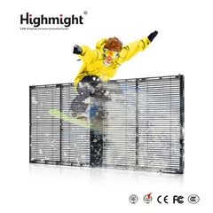
At Highmight, we believe that LED special-shaped screens are not only technological innovations, but also the evolution of artistic and commercial expressions. It breaks through the physical limitations of traditional screens, seamlessly integrates digital content into three-dimensional space, and makes each screen an intelligent interface connecting the physical and digital worlds.
For brands, Highmight's special-shaped screen technology provides a powerful narrative language - through customized shapes and dynamic content, brand stories can reach the audience in a more impactful way; for artists and designers, it is a canvas for releasing creativity, transforming abstract concepts into interactive visual experiences; for audiences, it means the arrival of an immersive sensory revolution.
In this era of visual supremacy, Highmight redefines the essence of "screen": it is no longer a static display tool, but an intelligent surface that can perceive the environment and interact with people. From commercial spaces to art installations, from building facades to product design, our technology is constantly expanding the dimensions of display - because true innovation always starts with "the possibility of imagination."


